
SPI
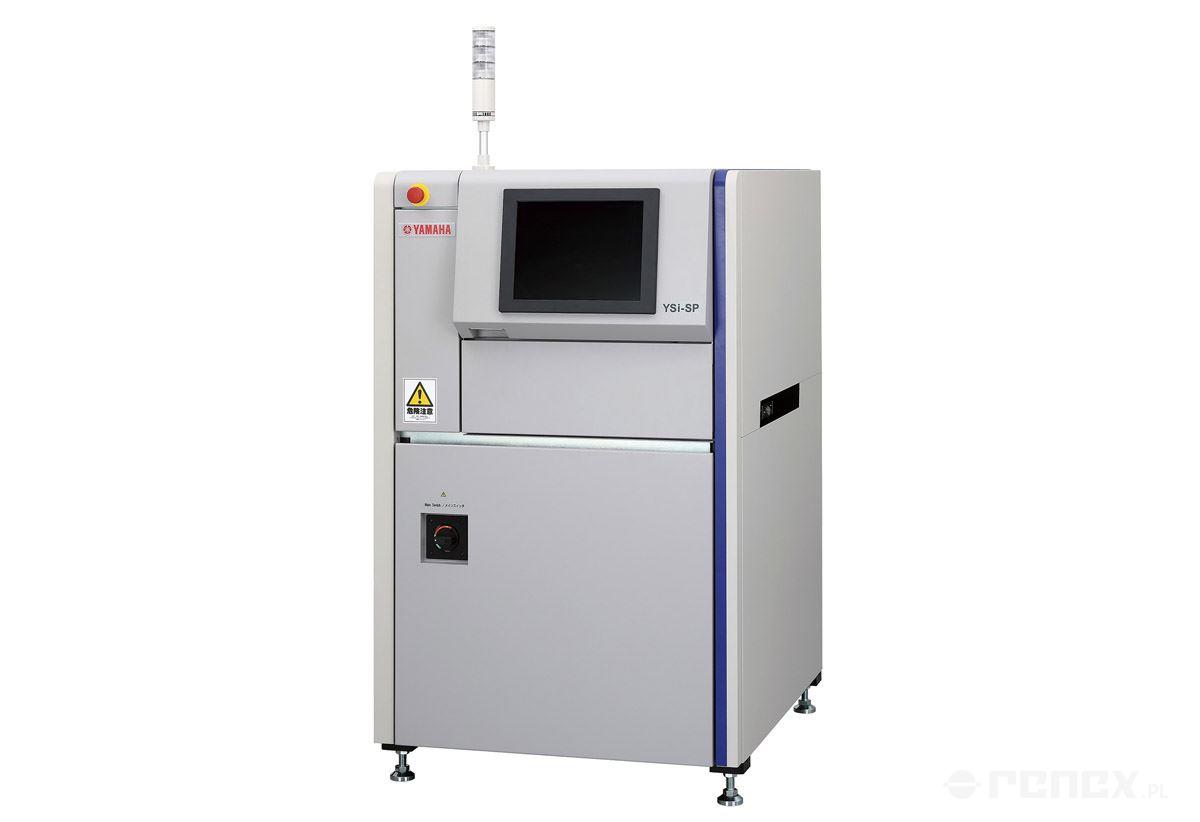
Solder paste inspection systems
SPI systems (Solder Paste Inspection) are advanced devices designed for the automatic inspection of solder paste deposits on printed circuit boards (PCBs). This process enables manufacturers to precisely control the volume, height, shape, and position of solder paste applied during the printing stage, directly impacting the final product quality.
SPI equipment utilizes high-resolution 3D cameras and advanced optical measurement technologies to accurately analyze solder paste deposits. By measuring parameters such as height, area, volume, and alignment, SPI systems can detect printing defects at an early stage of production, significantly reducing the risk of downstream assembly failures.
The SPI inspection process begins with capturing multi-angle images of the solder paste print using structured light or angled projection systems to generate a precise three-dimensional representation of the PCB surface. Dedicated SPI software then compares the captured data with predefined reference models to identify deviations from the expected pattern.
SPI systems are capable of detecting a wide range of defects, including insufficient or excessive solder paste, uneven deposits, bridging, contamination, misalignment, and printing deformations. Early detection allows manufacturers to implement corrective actions before the reflow process, preventing costly rework, scrap, and production downtime.
Modern SPI machines offer high-speed, high-precision inspection, enabling the analysis of large production volumes within short cycle times. In addition, they provide valuable process feedback data that supports continuous improvement, process optimization, and higher production yields in SMT manufacturing environments.