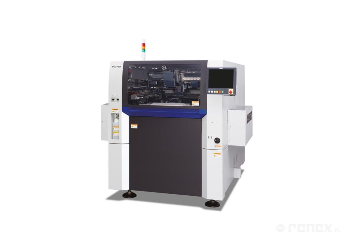
SEC X-eye 5100F X-ray inspection system
The SEC X-eye 5100F X-ray inspection system is an advanced device designed for non-destructive inspection of electronic components, semiconductors and SMT structures. Created for quality control, failure analysis and precise internal structural inspection, it offers excellent performance and image quality. At the heart of the system is a sealed micro-focus X-ray tube with 100 kV voltage and a 5 µm focal spot, working together with a high-resolution CMOS flat detector. This combination provides exceptionally sharp and detailed imaging even at high magnifications, making the X-eye 5100F an ideal tool for identifying micro-defects, solder voids, IC damage and discontinuities within material structures.
Advanced construction and multi-axis manipulator
The system is equipped with a multi-axis manipulator including X, Y, Z and rotational Tθ axes, enabling precise positioning of components at any angle. A large worktable measuring 340 × 460 mm allows convenient placement and handling of components of various sizes, while the wide motion range enhances inspection capabilities even for irregular shapes or parts located in hard-to-reach areas. The manipulator can be operated using a control panel with jog-stick joysticks or a mouse, providing full operational flexibility. Additionally, the system generates a vacuum level of 75%, equivalent to 570 mmHg and 22.4 inHg, stabilising the inspection process and enabling detailed imaging of enclosed components.
Maximum magnification of up to 130× enables evaluation of both broad structures and the finest details. External radiation below <1 µSv/h allows safe operation even during extended inspection sessions.
Operating software and automation functions
The X-eye operating software ensures comfortable use thanks to an intuitive interface and a rich set of measurement tools. The system supports CNC auto-learning, automatic BGA inspection with precise voiding analysis, image analysis tools, result mapping, annotation functions and real-time operation. The user can save settings, manage permissions, utilise automatic histograms and apply filtering functions that eliminate image distortions.
All of this is complemented by a user-friendly working environment that simplifies operation, ensures easy maintenance and allows system expansion with additional features depending on needs and budget.
SEC X-eye 5100F Technical Specifications
| Parameter | Value |
|---|---|
| Tube type | Sealed micro-focus 100 kV tube, 5 µm focal spot |
| Current | Max. 200 µA |
| Working vacuum | 75% / 570 mmHg / 22.4 inHg |
| Detector | CMOS flat detector |
| Magnification | Max. 130× |
| Manipulator | 4-axis: X, Y, Z, Tθ |
| Control | Jog-sticks or mouse |
| Motion range | X axis: 420 mm, Y axis: 300 mm, tilt T: ±45° |
| Worktable | 340 × 460 mm |
| External radiation | <1 µSv/h |
| Analysis | Real-time |
| Operational functions | Parameter saving, image filtering, histogram, annotations, auto-learning |
| Automatic BGA inspection | Yes, with voiding analysis |
| Processor | Intel® Xeon E3-1225 v3 @ 3.20 GHz |
| RAM | 8 GB |
| Drives | 2 × HDD 500 GB |
| Monitor | 24″ LCD |
| Operating system | Microsoft Windows 7 |
| Power supply | 220 VAC 50/60 Hz |
| Device dimensions | 1300 × 1000 × 1500 mm |
Applications of the SEC X-eye 5100F system
The system is used for analysing internal structures of electronic components, SMT assembly inspection, BGA void detection, diagnosis of through-hole component failures, evaluation of IC quality and semiconductor structure, inspection of plastic components and sealed modules, wire bond control and multilayer element evaluation. Thanks to its high image resolution and automation functions, it performs well in production departments, service environments and R&D facilities where precision and full reliability of results are required.
The SEC X-eye 5100F X-ray inspection system combines the high output of a micro-focus tube, an advanced CMOS detector and a multi-axis manipulator with versatile software offering automatic analytical functions, creating a complete platform for non-destructive inspection of electronic and semiconductor components. With real-time operation, detailed voiding analysis and easy operation, the system provides full diagnostic and quality-control capability, enabling detection of voids, discontinuities and micro-defects in the most demanding technological applications.